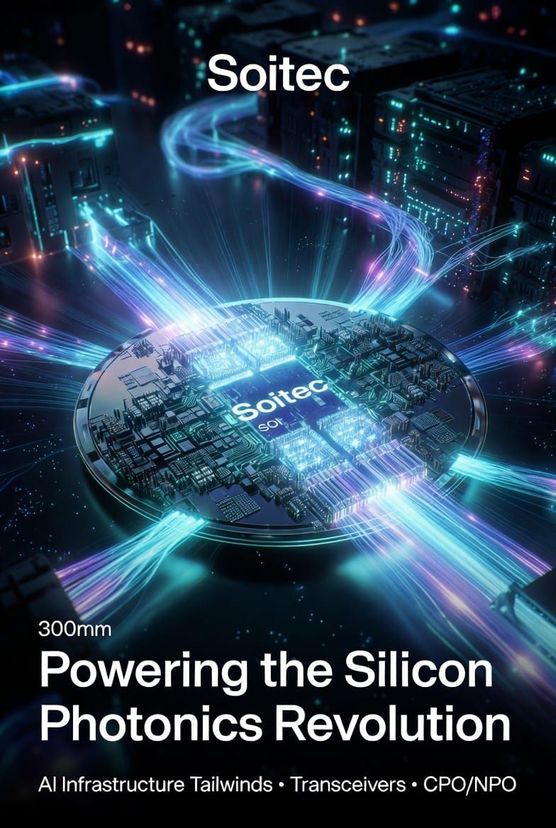
Soitec - Where Silicon Photonics Begins
The near-monopoly on Photonics-SOI wafers that every leading silicon photonics foundry depends on as the starting material for AI’s optical interconnect boom.
Summary
- Near-monopoly on Photonics-SOI, the engineered wafer every leading silicon photonics foundry depends on as starting material.
- Five compounding demand layers — cluster scale, optics-per-accelerator, SiPho share gains, scale-up optics, and memory disaggregation — all converging on the same wafer.
- SiPho is becoming the default, winning on cost and volume today and closing the performance gap with InP/EML at 1.6T and 3.2T.
- Pluggables → NPO → CPO is an intensification, not a substitution, with each step increasing silicon area per system.
- A dynamic moat via Smart Cut and the Photon → Photon Plus → Photon Ultra roadmap, already co-developed against CPO-era customer specs.
Intro
In our last Notes we introduced POET Technologies and its Optical Interposer — a platform that integrates lasers, detectors, and waveguides into a single chip-scale optical engine. POET builds its interposer on standard bulk silicon, deliberately avoiding specialised substrates to enable low-cost, CMOS-compatible manufacturing. Soitec occupies a different, upstream position in the supply chain: it produces the specialised Photonics-SOI (Silicon On Insulator) engineered wafers that every silicon photonics foundries require as starting material for high-performance optical circuits. Both companies stand to benefit from the same AI-driven optical build-out, but in distinct and complementary ways.
The Surging Demand for SiPho
To understand Soitec's positioning, you have to understand why silicon photonics (SiPho) demand is accelerating so sharply — and why this acceleration has multiple, compounding layers.
The starting point: an InP/EML supply crunch
Today, most optical transceivers are built using Indium Phosphide (InP) substrates with Electro-absorption Modulated Lasers (EMLs) integrated directly into the laser chip. EML-based transceivers have historically offered the best raw performance for high-speed pluggables.
The problem is that the InP and EML supply chain was never built for AI-scale demand. InP is a III-V compound semiconductor produced in much smaller wafer sizes and lower volumes than silicon. EML fabrication is complex, low-yielding, and concentrated in a handful of suppliers. Lumentum — one of the dominant EML providers — has its own well-documented capacity bottlenecks. The result is multi-quarter lead times for InP wafer delivery into foundries, and an optical transceiver market that is now genuinely supply-constrained at exactly the moment AI is demanding orders of magnitude more units.
This is the catalyst that has tipped the industry toward silicon photonics.
The pivot: SiPho as the only scalable answer
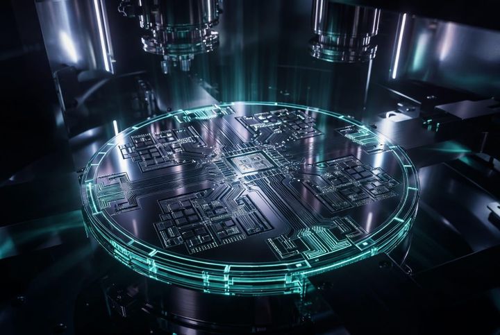
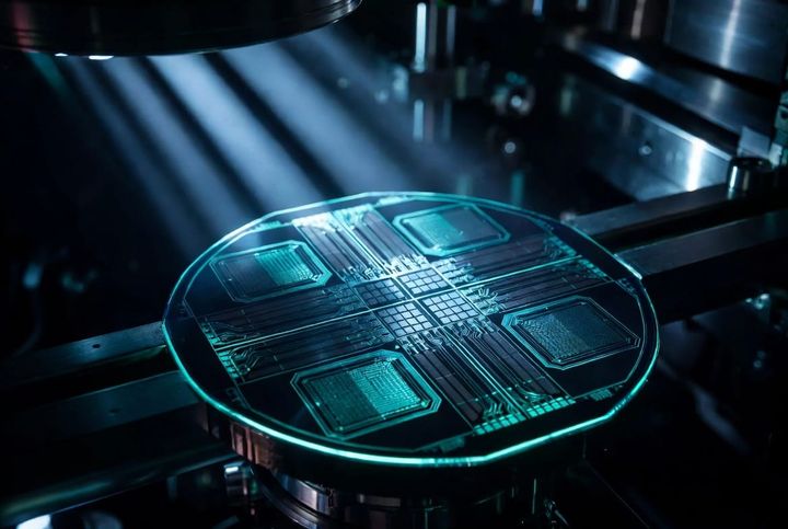
SiPho transceivers use a separate continuous-wave (CW) laser (still typically on InP, but a far simpler device than an EML) paired with a Photonic Integrated Circuit (PIC) built on a Photonics-SOI wafer (made by Soitec) for waveguides, modulators, and detectors.
Historically, SiPho was viewed as the cheaper, lower-performance option — adequate for many use cases but not the premium choice. That framing is now being rewritten in real time:
- Cost: SiPho leverages CMOS infrastructure and 200/300mm wafers, dramatically lowering unit cost.
- Volume: Silicon photonics foundries (TSMC, GlobalFoundries, Tower, Intel) can scale capacity in ways InP simply cannot.
- Performance: This is the part most observers underweight. Tower's upcoming introduction of silicon-germanium hybrid bonding materially closes the performance gap with InP/EML — and at higher data rates may surpass it.
If SiPho becomes not just the cost and volume leader but also a performance leader, the industry has every reason to standardise on it. And as we approach 3.2T transceivers, current InP/EML technology runs out of headroom — the industry will need either D-EMLs (still emerging and capacity-constrained) or SiPho with silicon-germanium. The latter path clearly points toward more Photonics-SOI demand, while D-EML adoption would still rely on SiPho-based receivers (Ge-on-Si photodetectors) in most hybrid designs.
The adoption curve is already steep. Innolight's management commentary — a useful proxy for the broader market — implies SiPho went from ~20% of optical transceivers in 2025, to ~50% today, with a path to ~70% by 2027.
The five layers of demand stacking on Soitec
This is where the investment case becomes more powerful than a single tailwind. There are at least five compounding demand drivers, each independently meaningful, all pulling in the same direction:
Layer 1: AI clusters are getting bigger. A 100k-GPU cluster requires far more optical transceivers than a 10k-GPU cluster — not linearly, but super-linearly, because the network fabric scales with the square of the node count in many topologies. Cluster size alone is a multi-year tailwind for transceiver volume.
Layer 2: More transceivers per ASIC/GPU. As bandwidth-per-accelerator climbs (Nvidia's roadmap is the clearest example), the number of optical lanes per chip is rising. Each generation packs more optics around the same compute die.
Layer 3: SiPho taking share from InP/EML. As discussed above — already underway, accelerating, with Innolight's 20% → 50% → 70% trajectory as the reference point.
Layer 4: SiPho extending into scale-up via NPO and CPO. Today's optical transceivers are largely a scale-out phenomenon (connecting servers and racks). Scale-up — the ultra-high-bandwidth domain inside a single accelerator complex — has historically been copper. As bandwidth requirements outrun copper's reach, optics is moving inside the package. If SiPho also wins on performance, it unlocks a vastly larger scale-up TAM that copper is currently failing to serve.
Layer 5: Memory pooling. This is the most underappreciated driver. As models grow, the "memory wall" becomes the binding constraint — individual GPUs don't have enough HBM, and replicating memory across nodes is wasteful. The architectural answer is disaggregated memory pools: a shared pool of memory accessed by many accelerators over optical links. For this to work, you need extremely high-bandwidth, low-latency optical interconnects between compute and memory — exactly what SiPho/CPO enables. Memory pooling effectively creates a new category of optical transceiver demand on top of traditional networking, and it scales with model size, not just cluster size.
From pluggables to CPO — and why NPO matters
The long-term industry direction is to move the electrical-to-optical conversion ever closer to the ASIC. Pluggables sit 10–30cm away. Co-packaged optics (CPO) brings the photonic engine into the same package as the ASIC, collapsing electrical reach from centimetres to millimetres and dramatically reducing power, latency, and SerDes complexity.