Notes: The Bottleneck Heuristic — Blackwell's Gauntlet, the ASIC Breakout, and the Optical Chokepoint (Pt.2)
Blackwell’s packaging, cooling, NVL72, and on-chip SFU bottlenecks exposed NVDA’s gauntlet — while Google’s AVGO-designed TPUv7 shattered the ASIC skepticism and the optical chokepoint tightened into 2025’s defining constraint.
Summary
- Following Part 1's investment heuristics, Part 2 recaps the pivotal developments of 2024–25, starting with NVDA's Blackwell — delayed ~9–12 months by packaging respins, liquid-cooling redesigns, NVL72 reliability issues, and an on-chip SFU bottleneck.
- Google's TPUv7 (AVGO-designed) shattered the "ASICs can't train" consensus by powering Gemini 3 Pro past GPT-5 and cutting Anthropic's token costs ~3x — the custom ASIC breakout moment investors can no longer dismiss.
- MSFT's Maia (MRVL) and AMZN's Trainium underscore the cost of skimping on design partners — both delivered worse performance at higher total cost, while Meta, SoftBank, and others now flock to AVGO.
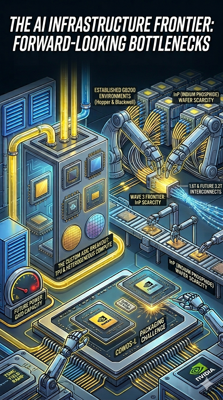
- Turning to the forward view, NVDA's NVL576 marks a pivotal optical pivot, but collides with a severe InP laser bottleneck; SiPho is the key solver, and TSEM — the only foundry qualified at 1.6T — plans ~5x capacity expansion in 2026.
- The competitive landscape is bifurcating: NVDA must defend its training TAM through system-level integration while AVGO, TSEM, and SiPho-enabled transceiver makers emerge as structural winners in the next infrastructure wave.
Wave 2: The Blackwell Bottleneck and Execution Gauntlet (2024–2025)
Massive GPGPU demand left NVDA both empowered and exposed. The company couldn't simply ramp production of existing chips — it had to accelerate delivery of dramatically superior next-generation products. The strategic logic was straightforward: if customers remained GPU-starved for too long, they would be forced to invest more seriously in alternative architectures — AMD's MI300X, Intel's Gaudi 3, Google's TPUs, various custom ASICs — and once those alternatives gained a foothold, even a narrow one built on better perf/$ claims in specific workloads, they could expand over time. NVDA's dominance depended on keeping the performance-per-dollar frontier moving fast enough that no competitor could close the gap.
This created something like the innovator's dilemma in reverse. In Christensen's classic formulation, incumbents fail because they rationally refuse to cannibalize their own profitable products, leaving the door open for cheaper, "good enough" alternatives to enter from below and eventually displace them. NVDA faced the same threat landscape — scrappy alternatives circling beneath a dominant product line — but responded in the opposite way. Rather than protecting Hopper-era margins and hoping the moat would hold, NVDA moved to cannibalize its own lineup as aggressively as possible, racing to obsolete its current generation before competitors could catch up to it.
As a result, NVDA rushed to bring Blackwell into production on an aggressive timeline and explored novel "SysMoore" architectural approaches to maximize performance gains across the entire system — not just at the chip level, but at the rack, cluster, and data center level. Jensen Huang's vision was that Moore's Law at the individual chip level was slowing, but "system-level Moore's Law" could continue if you co-optimized silicon, packaging, interconnect, cooling, power delivery, and software simultaneously. It was an ambitious thesis, but the execution proved to be extraordinarily challenging.
The Packaging Challenge. It turned out that Blackwell had significant problems across multiple dimensions. Starting with the chip package itself: Blackwell represented NVDA's first deployment of a chiplet-based design for a GPU, departing from the monolithic die approach that had defined every prior NVDA GPU architecture. The B200 die consisted of two GPU compute chiplets connected via a high-bandwidth die-to-die link, packaged together with HBM stacks on a single substrate. To achieve the best-in-class chiplet interconnect — with bandwidth and latency approaching what a monolithic die would deliver — NVDA chose to use TSMC's novel CoWoS-L (CoWoS with Local Silicon Interconnect) advanced packaging technology, rather than the more established CoWoS-S.
CoWoS-L was, at the time of Blackwell's tape-out, still in its early qualification phase at TSMC. It used a local silicon interconnect (LSI) bridge — a small piece of silicon embedded in the organic substrate — to provide ultra-high-bandwidth die-to-die connectivity between the two GPU chiplets. The technology offered substantial advantages in terms of package size, signal integrity, and bandwidth density, but it was significantly less mature than CoWoS-S. The initial tape-out revealed a design error related to the die-to-die interconnect interface, reportedly involving signal integrity issues at the LSI bridge that caused yield problems. Both NVDA and TSMC had to go back and engineer a workaround, which involved mask revisions and process adjustments that consumed approximately 4-6 additional months. During this period, TSMC also had to simultaneously ramp up CoWoS-L production capacity from an engineering-sample scale to high-volume manufacturing — a parallel effort that further strained resources and engineering capacity.
The Rack-Level Complexity. Beyond the chip package, Blackwell's system-level architecture represented a quantum leap in complexity. To deliver a much larger scale-up domain of 72 GPUs (in the NVL72 configuration) instead of the 8-GPU DGX H100 scale-up domain, NVDA designed a novel rack-level system that connected 36 dual-GPU nodes (each containing two B200 dies) into a single rack, with all 72 GPUs sharing a unified memory space via 5th-generation NVLink. This rack consumed approximately 120kW of power — effectively 10x the power density of a previous-generation CPU rack and roughly 4x the power of an H100-based DGX rack.