Notes: ASM and the Rising Complexity of Chips & Why ALD Matters More Than Ever
Summary
- Semiconductor scaling is shifting from lithography alone to materials precision and 3D architectures, structurally increasing ALD intensity where ASM is strongest.
- The transition to GAA, backside power delivery, and 2nm-class nodes creates a multi-year growth cycle driven by process complexity rather than wafer volume.
- AI-driven demand is expanding ALD exposure beyond logic into HBM, advanced packaging, and increasingly logic-like memory architectures.
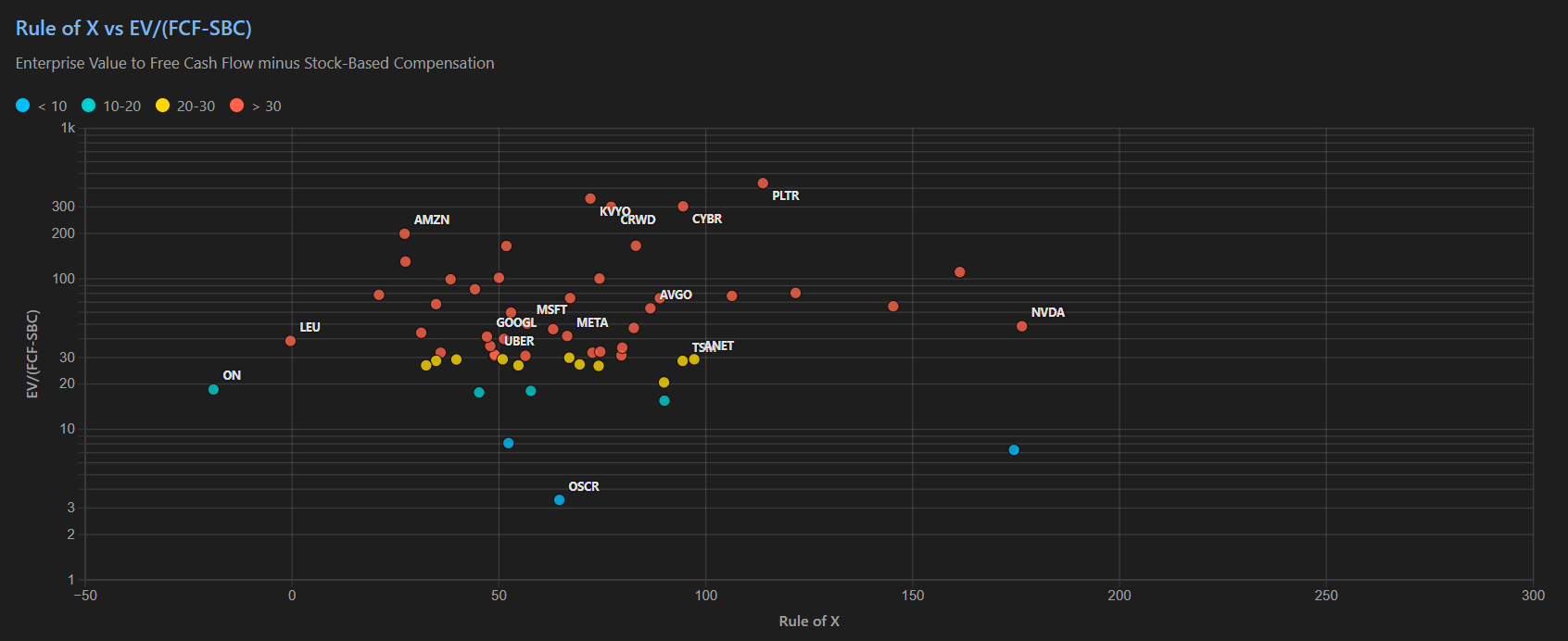
- Near-term results depend on 2026 spending mix, but tight 2nm capacity, rising memory pricing, and supply constraints point to a potentially stronger WFE upcycle.
- ASM appears fairly valued today, but if ALD becomes a critical scaling bottleneck, the company could re-rate toward premium WFE leaders over time.
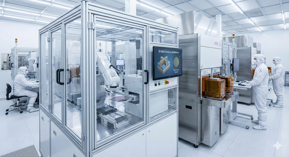
ASM sits at the center of a structural shift in semiconductor manufacturing. As lithography continues to push transistors to ever-smaller geometries, the margin for error in materials engineering is shrinking, increasing the need for atomic-level control over film thickness, uniformity, and interfaces. At the same time, performance gains are increasingly being driven by three-dimensional architectures — first at the transistor level through structures such as GAA and backside power delivery, and then at the die level through stacking, TSVs, hybrid bonding, and broader 3D integration to increase effective silicon density.
Both trends — continued dimensional scaling and the expansion of transistor-level and die-level 3D — rely on highly precise, conformal deposition across complex and high-aspect-ratio structures in logic as well as DRAM, HBM, and NAND. This makes ALD a foundational process for advanced chip manufacturing, a dynamic that plays directly into ASM’s core strengths in ALD and selective epitaxy.